RF PCB Design
RF (Radio Frequency) signals require high-performance PCBs to ensure that they are transmitted without loss. These PCBs must be designed according to strict guidelines in order to prevent signal reflections, electromagnetic interference, and capacitive coupling between two major signals. This requires the use of specialized circuit board materials that are designed for RF applications. These include RF ceramics, which offer exceptional thermal, electrical and mechanical properties. They also provide superior RF performance and are suitable for applications that require conformal electronics.
RF PCBs are multi-layered boards that feature different copper layer thicknesses, conductor widths and dielectric constants to ensure maximum functionality. The most important parameter for RF PCBs is the characteristic impedance, which is the ratio of the voltage and current of the wave that travels along the transmission line. This value is determined by the type of material, trace width and thickness, and clearance between the traces and ground fill. It is also affected by the circuit layout, so it is important to follow RF PCB design guidelines carefully.
The first step in rf pcb design is to choose the right substrate for the project. Depending on the performance indicators of the circuit, it can be made from a standard FR4 epoxy glass laminate or a special microwave substrate like Teflon. Using the right substrate helps to avoid skin effect, which is the increase in power losses as the frequency of the signal increases.
How RF PCB Design Enables Conformal Electronics
Next, the RF design requires impedance matching, which is done by installing a network near the RF source and load to match their characteristic impedance. This is essential, because the higher the frequencies are, the less tolerant they are of variations in impedance. Ideally, the RF PCB should have no more than 50 ohms of impedance between the source and load, but this can be difficult to achieve because it is a complex issue.
An RF pcb design must also consider the size of the antenna, which can be as small as an IoT sensor or as large as a satellite. The size of an antenna depends on the needs of the product, but larger antennas provide better signal strength and longer communication range. It is recommended that the RF traces be placed close to each other, but they should be separated from the non-RF parts by at least 2cm to prevent interference.
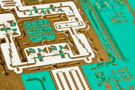
The choice of the RF PCB layers is another critical decision, as it will affect the overall performance of the circuit board. Typically, the outer layers are thicker Rogers core materials, while the inner layers are bondply layers that function as prepregs in traditional PCB stack-ups. This allows the RF layers to remain as flat as possible, reducing attenuation and improving signal quality. This stackup style can be seen in the example shown below.